 Techcomp headquarters
  Techcomp regional offices
  Manufacturing, design and R&D facilities

product
- Atomic Force Microscope
- FE-SEM
- Hi-SEM
- Optical Interferometry System
- Sample Preparation
- Tabletop Microscope
- Transmission Electronic Microscope
- X-Ray Spectroscopy
- Fluorescence Spectrophotometer
- Amino Acid Analyzer
- Atomic Absorption Spectrophotometer
- Autotitrator
- Mercury Analyzer
- UV-VIS Spectrophotometer
- High Performance Liquid Chromatography
- Thermal Analyzer
- Automatic Moisture and Ash Content Analyzer
- Fluorescence Spectrophotometer
- Fluorescence Steady State & Life Time / Flash Photolysis
- Mercury Analyzer
- Raman Spectroscopy
- UV-VIS Spectrophotometer
- Mass Spectrometer
- FTIR Spectrometer
- Chromatography Data System
- Gas Chromatography
- Gas Chromatography-Mass Spectrometer (GC-MS)
- Liquid Chromatography
- Sampler and sample pretreatment system
- Column and Consumable
- Amino Acid Analyzer
- Anaerobic & Hypoxic Chambers
- Autoclave & Sterilization
- Biological Safety Cabinets & Clean Benches
- Blood bank & Phamacy Freezer
- Cryopreservation Systems
- DNA & RNA Purification
- Environmental Chambers
- Freezer Dryer
- High Capacity Centrifuge
- High Speed Centrifuge
- Lab Water Purification
- Lab Oven & Incubator
- Life Science
- Mixer
- Pipette
- Tabletop Centrifuge
- Ultracentrifuge
- ULT Freezer
- Temperature Forcing System
- Precisa Analytical Balances
- Precisa Micro Balances
- Precisa Precision Balances 0.001g
- Precisa 520 PB/PT Analytical and Precisa balances
- Preicsa 320 XB Series Balances
- Precisa 165 BJ Series Balances
- Precisa 410 SRS/SRC Series Scale
- Precisa 365 EM/330 XM Moisture Analyzers
- Precisa 490 Series Industrial Scales
- Precisa 321 LX/LS-STB Series Stirrer Balances
- Precisa 321 LG Series Balances
- Standard Balances
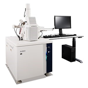
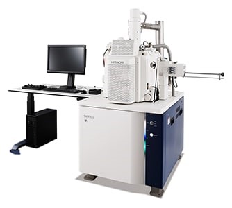
Scanning Electron Microscopes SU3800/SU3900
Hitachi electron microscopes SU3800/SU3900 deliver both operability and expandability. The operator can automate many operations and efficiently utilize their high performance. The SU3900 is equipped with a large multipurpose specimen chamber to accommodate observation of large samples.
Download- Hong Kong SAR
Hitachi Scanning Electron Microscopes SU3800/SU3900
The modern SEMs must be highly versatile and easy to use for all experience levels. Hitachi SU3800/SU3900 were designed to address these needs and more, Hitachi High-Technologies provides a novel solution with the SU3800/SU3900. Advanced automation functions including auto start, wide-angle camera navigation with stitching, and auto algorithms enable high-throughput, easy-to-use systems for both new and experienced operators. The oversized SU3900 features a class-leading specimen chamber/stage configuration with ability to accommodate a 300-mm sample diameter and loading capacity up to 5 kg. This allows for easy observation of very large samples without the need to cut or process prior to imaging
Main Features
(1) Handles large, heavy specimens
- The SU3800 can accommodate a specimen up to a 200-mm diameter with maximum height of 80 mm and weight of 2 kg.
- The SU3900 can accommodate a specimen up to a 300-mm diameter with maximum height of 130 mm and weight of 5 kg.
(2) Support for wide-area observations
- SEM MAP with camera navigation supports quick ROI targeting from wide-angle optical image.
- Multi Zigzag function allows for multi-frame stitch acquisition at user-selectable regions of interest, even from SEM MAP optical image.
(3) Improved operation through automation
- The automatic function for image adjustment reduces waiting time from start to acquisition.
- Intelligent Filament Technology (IFT) software automatically monitors and controls filament conditions as well as indicates the remaining filament life. This is advantageous for continuous observation over a long period of time or wide-area particle analysis.
Main Specifications:
|
Items |
|
Description |
|
Secondary Electron Image Resolution |
3.0 nm (Accelerating Voltage: 30 kV, high vacuum mode) 15.0 nm (Accelerating Voltage: 1 kV, high vacuum mode) |
|
|
Backscattered Electron Image Resolution |
4.0 nm (Accelerating Voltage: 30kV, low vacuum mode) |
|
|
Accelerating Voltage |
0.3 to 30 kV |
|
|
Magnification |
×5 to ×300,000 (photo magnification) ×7 to ×800,000 (actual display magnification) |
|
|
Specimen Stage |
X: 0 to 100 mm Y: 0 to 50 mm Z: 5 to 65 mm T: -20° to 90° R: 360° |
X: 0 to 150 mm Y: 0 to 150 mm Z: 5 to 85 mm T: -20° to 90° R: 360° |
|
Maximum Loadable Specimen Size |
200 mm diameter |
300 mm diameter |
|
Maximum Observable Range |
130 mm diameter (with rotation) |
200 mm diameter (with rotation) |
|
Maximum specimen height |
80 mm (WD = 10 mm) |
130mm (WD = 10 mm) |
Product Video
Application: Metallic Materials, Ceramic Materials,
Electronic Materials, Biology/Pharmaceutical Materials

 2606, 26/F., Tower 1, Ever Gain Plaza, 88 Container Port Road, Kwai Chung, N.T., Hong Kong
 +852-27519488 / WhatsApp/WeChat HK: +852-8491 7250
 techcomp@techcomp.com.hk
 Sweep The Concern Us