 Techcomp headquarters
  Techcomp regional offices
  Manufacturing, design and R&D facilities

product
- Atomic Force Microscope
- FE-SEM
- Hi-SEM
- Optical Interferometry System
- Sample Preparation
- Tabletop Microscope
- Transmission Electronic Microscope
- X-Ray Spectroscopy
- Fluorescence Spectrophotometer
- Amino Acid Analyzer
- Atomic Absorption Spectrophotometer
- Autotitrator
- Mercury Analyzer
- UV-VIS Spectrophotometer
- High Performance Liquid Chromatography
- Thermal Analyzer
- Automatic Moisture and Ash Content Analyzer
- Fluorescence Spectrophotometer
- Fluorescence Steady State & Life Time / Flash Photolysis
- Mercury Analyzer
- Raman Spectroscopy
- UV-VIS Spectrophotometer
- Mass Spectrometer
- FTIR Spectrometer
- Chromatography Data System
- Gas Chromatography
- Gas Chromatography-Mass Spectrometer (GC-MS)
- Liquid Chromatography
- Sampler and sample pretreatment system
- Column and Consumable
- Amino Acid Analyzer
- Anaerobic & Hypoxic Chambers
- Autoclave & Sterilization
- Biological Safety Cabinets & Clean Benches
- Blood bank & Phamacy Freezer
- Cryopreservation Systems
- DNA & RNA Purification
- Environmental Chambers
- Freezer Dryer
- High Capacity Centrifuge
- High Speed Centrifuge
- Lab Water Purification
- Lab Oven & Incubator
- Life Science
- Mixer
- Pipette
- Tabletop Centrifuge
- Ultracentrifuge
- ULT Freezer
- Temperature Forcing System
- Precisa Analytical Balances
- Precisa Micro Balances
- Precisa Precision Balances 0.001g
- Precisa 520 PB/PT Analytical and Precisa balances
- Preicsa 320 XB Series Balances
- Precisa 165 BJ Series Balances
- Precisa 410 SRS/SRC Series Scale
- Precisa 365 EM/330 XM Moisture Analyzers
- Precisa 490 Series Industrial Scales
- Precisa 321 LX/LS-STB Series Stirrer Balances
- Precisa 321 LG Series Balances
- Standard Balances
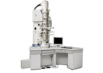
Field Emission Transmission Electron Microscope
The HF-3300 is a 100-300 kV TEM/STEM/SEM powered by Hitachi's state-of-the-art cold field emission technology for high-brightness and high-energy resolution. Capabilities needed for daily material structural characterizations and analysis are provided. Unique electron optical designs include spatially resolved EELS and double biprism electron holography (special order). The simultaneous secondary electron imaging and STEM imaging reveal surface and bulk structures at the same time. A special version for gas environmental TEM or aberration-corrected microscopy is available.
Download- Hong Kong SAR
Hitachi Field Emission Transmission Electron Microscope HF-3300
Transmission Electron Microscope is an essential instrument in surface science. Hitachi HF3300 is a high resolution transmission electron microscope for most materials (metals, ceramics, etc.) samples. It can simplify the sample preparation, ensure high resolution, and also meet the requirements of high spatial resolution analysis. With the combination of EELS and nanobeam diffraction function, the distribution of nanoscale elements and crystal structure can be studied. The unique analytical capabilities and user-friendly operation also greatly expand its application fields.
Features:
· High-brightness Cold Field Emission (Cold FE) electron source
Cold field emission electron source benefits nanoscale analysis with its high brightness and high-energy resolution. Its inherent high coherency greatly contributes to ultra-high resolution imaging and electron holography.
· 300 kV accelerating voltage
A 300 kV accelerating voltage allows atomic-resolution imaging for thick specimens. Metals and ceramics with high atomic numbers are less electron transparent and often need to be observed at a 300 kV accelerating voltage.
· Unique analytical capabilities
The newly introduced spatially resolved EELS and the in-situ SEM/TEM imaging nanobeam electron diffraction provide sophisticated and unique analytical capabilities.
· Holder linkage with the FIB system
The Hitachi-FIB-compatible specimen holder requires no tweezer handling of TEM grids between FIB fabrication and TEM observation and ensures high-throughput TEM analysis. Hitachi's unique specimen rotation holder enables real-time multidirectional structural analysis together with an STEM unit.
· User-friendly operation
Windows-based TEM/STEM computer control, a motor-driven movable aperture, and a 5-axis motorized stage make the high-end TEM more accessible. It only takes 10 minutes to be high-voltage-ready and 1 minute for specimen exchange, providing high sample throughput for TEM analysis.
Specifications:
|
Items |
Description |
|
|
Electron source |
W(310) cold field emission electron source |
|
|
Accelerating voltage |
300 kV, 200 kV*2, 100 kV*2 |
|
|
Resolution |
Lattice |
0.10 nm |
|
Point-to-point |
0.19 nm |
|
|
Information limit |
0.13 nm |
|
|
Magnification |
Low Mag mode |
200 - 500× |
|
High Mag mode |
2,000 - 1,500,000× |
|
|
Image rotation |
±5° or less (High Mag mode, below 1,000,000×) |
|
|
Specimen tilt |
±15° |
|
|
Camera length |
300 - 3,000 mm |
|
Application: Material Science, Semiconductors

 2606, 26/F., Tower 1, Ever Gain Plaza, 88 Container Port Road, Kwai Chung, N.T., Hong Kong
 +852-27519488 / WhatsApp/WeChat HK: +852-8491 7250
 techcomp@techcomp.com.hk
 Sweep The Concern Us